Figure 5.
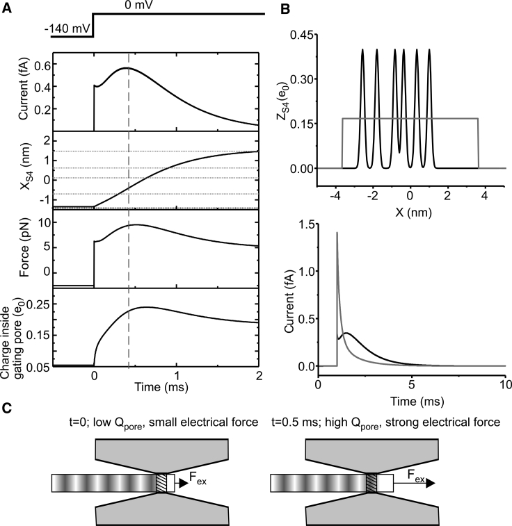
(A) Time courses of (from top to bottom) the gating current, the mean position of the S4 segment (xS4) obtained as , the force acting on the S4 segment, and the gating charge residing inside the gating pore. The VSD was subjected to a depolarization from −140 to 0 mV (voltage protocol indicated above the plots). (B) S4 segment charge profiles (upper graph) and gating currents obtained in response to a depolarization from −140 to 0 mV (lower graph), for our model (black lines) and for a model in which the gating charge density over the S4 segment region traversing the gating pore during activation was made homogeneous (gray lines). Notice that the rising phase of the gating current disappears when considering a homogeneous charge density along the S4 segment. (C) A drawing is given showing that upon depolarization, the R1 charge enters the gating pore, causing an increase in the force acting on the voltage sensor.

