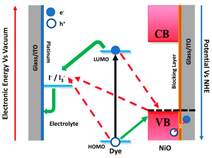
Scheme 1.
Scheme of the electronic process occurring in a p-DSC. The black line corresponds to the light-induced photoexcitation; green lines schematize the electrons (and holes) in an ideal device. Red lines accounts for undesired recombination reactions. The implementation of a blocking layer minimizes the recombination between the holes in the NiO VB and the electrons in the ITO layer.

