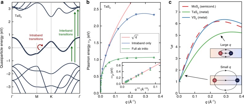
Fig. 1. Plasmon dispersion relation of an atomically thin quasi-2D crystalline metal.
a Calculated GW quasiparticle band structure of a prototypical quasi-2D metal, monolayer TaS2. The arrows highlight the intraband and interband electronic transitions that contribute to a plasmon excitation. The Fermi energy is set at zero. b Calculations of the plasmon dispersion relation of monolayer TaS2. The green curve is the result of the full ab initio calculation, which displays a flattening of the plasmon dispersion relation; the blue curve corresponds to the result of a calculation including only the intraband transitions, which displays a dispersion relation much closer to ~ (red curve). The inset shows the small-q behavior of the plasmon dispersion relation, where both calculations follow a dependence. c Effective 2D dielectric function εeff(q) for two point charges located at the innermost portion of three different quasi-2D materials. Since εeff(q) does not include intraband (but only interband) transitions, its behavior is similar to quasi-2D semiconductors. For very small wavevectors, there is no screening (εeff(q = 0) = 1)) since very long wavelength perturbations correspond to charges being so far apart that they only experience the screening of vacuum. For increasing wavevector q, the charges get closer, so more of the field lines connecting them are confined to the interior of the quasi-2D material. εeff(q) increases linearly with q until it reaches near a maximum, and subsequently decreases with increasing q after the maximum due to the intrinsic inability of the medium to screen very short-wavelength excitations.

