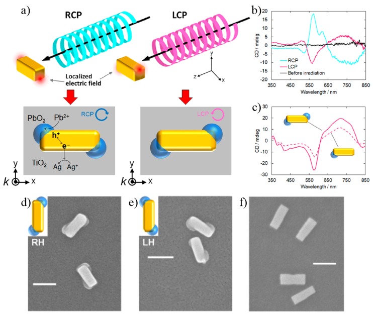
Figure 7.
(a) Illustration of the deposition of a dielectric material (PbO) via Pb oxidation under CPL stimulus. (b) Substrate CD before the dielectric material deposition (black line) and after deposition under RCP (blue line) and LCP (red line) lights. (c) Comparison of CD spectra of a left-handed nanocuboid with one and two PbO. SEM images of a right-handed (d), a left-handed (e) and before deposition (f) nanocuboids. Reproduced with permission from ref. [80]. Copyright 2018 American Chemical Society.

