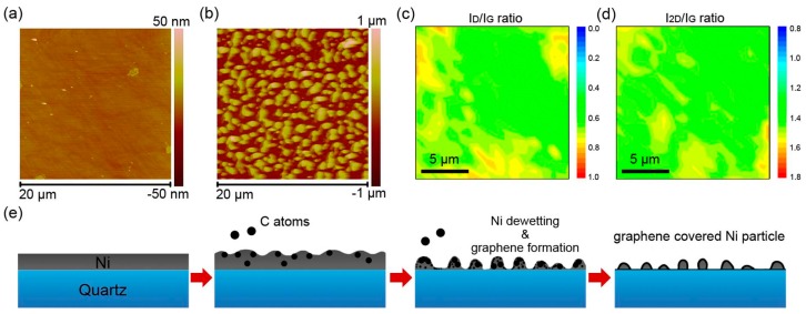
Figure 3.
(a,b) Atomic force microscope (AFM) images of the surface morphology of as-deposited Ni layer and after Ni/G electrodes. (c,d) Raman mapping of Id/IG ratio and I2D/IG ratio of (b). (e) Scheme of change of surface morphology and graphene fabrication during the plasma-enhanced chemical vapor deposition (PECVD) process.

