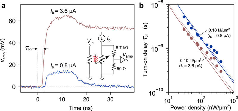
Figure 3.
Driving an 8.7 kΩ load using the switch. (a) Output produced by a 10-ns-wide square pulse to the heater with input surface power density D = 50 nW/μm2, highlighting the latching and non-latching regimes. Trace data taken with a 1 GHz bandwidth-limited amplifiers and oscilloscope. (b) Turn-on delay τ on versus applied input power when the nanowire is biased below the retrapping current (blue) and near Ic (red). The solid lines are fits generated by the ballistic phonon transport modeling, and the dotted lines are constant-energy per unit area curves corresponding to 0.18 fJ/μm2 (blue) and 0.10 fJ/μm2 (red).

