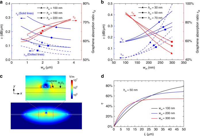
Fig. 2. Mode properties of the present silicon−graphene hybrid plasmonic waveguide when operating at λ = 2 μm.
a Calculated absorption coefficients (αg, αm) and the graphene absorption ratio ηg as the silicon ridge width wsi varies for cases with different silicon ridge heights hsi. Here, wm = 200 nm, and hm = 50 nm. b Calculated absorption coefficients (αg, αm) and the graphene absorption ratio ηg as the metal strip width wm varies for cases with different metal heights hm. Here, wsi = 3 μm, and hsi = 100 nm. c The electric field component distribution of the quasi-TE0 mode for the optimized silicon−graphene hybrid plasmonic waveguide. d Calculated graphene absorptance η as the propagation length L varies for cases with different metal widths of wm = 100, 200, and 300 nm. Here, hm = 50 nm, wsi = 3 μm, and hsi = 100 nm

