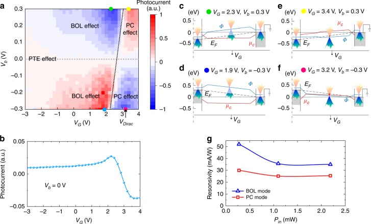
Fig. 3. Static characterization of the present silicon−graphene hybrid plasmonic waveguide photodetector (Device A).
a Measured photocurrent map as the gate voltage VG and the bias voltage Vb vary. b Dependence of the photocurrent at zero bias for the gate voltage VG. c−f Calculated energy band diagrams for the cases of (VG, Vb) = (2.3, 0.3), (1.9, −0.3), (3.4, 0.3), and (3.2, −0.3) V. g Measured responsivities with different input optical powers Pin. Here, Vb = −0.3 V and VG = ~1.9 V (for the BOL effect), or VG = ~3.2 V (for the PC effect)

