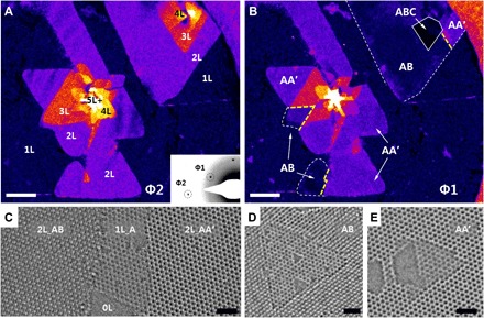
Fig. 1. TEM images of few-layer AA′- and AB-stacked hBN films.

(A and B) False-color DF-TEM images of triangular, few-layer hBN islands from (A) a Φ2 diffraction spot [inset of (A)] and (B) a Φ1 diffraction spot [inset of (A)]. In (A), the number of layers (1L to 5L+) is identified, while different stacking structures (AA′, AB, and ABC) are shown in (B). (C to E) HR-TEM images of AA′- and AB-stacked hBN. Triangular defects grow in the same orientation in AB-stacked hBN (C) and in the opposite direction in AA′-stacked hBN (E). Scale bars, 0.1 μm (A and B) and 1 nm (C to E).
