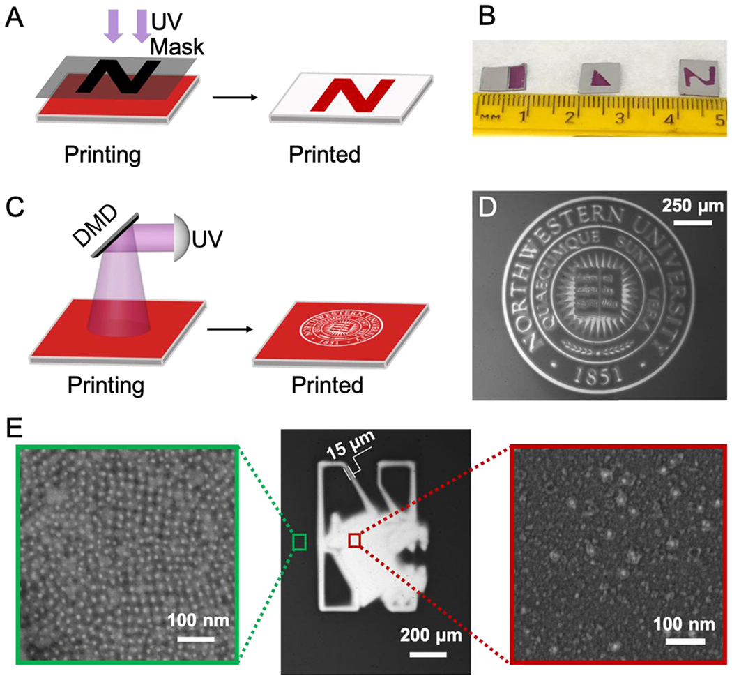
Figure 4.

(A) A custom-made photomask can be used to pattern crystalline PAE thin films into desired shapes. (B) Photograph showing photomask-patterned samples of three different shapes (rectangle, triangle, and the letter “N”). (C) A digital micromirror device (DMD) is used with a cantilever-free scanning probe lithography instrument to photopattern crystalline PAE thin films. (D) Optical microscope image confirms successful photopatterning of a predesigned image. (E) Optical microscope image (middle), with a zoomed-in SEM image confirming that PAEs remain intact and ordered on the area that was not exposed to UV light (left) and another zoomed-in SEM image showing sparsely distributed nanoparticles on the UV-exposed region and demonstrating that the majority of light-responsive PAEs are successfully removed from the substrate (right).
