
Figure 2.
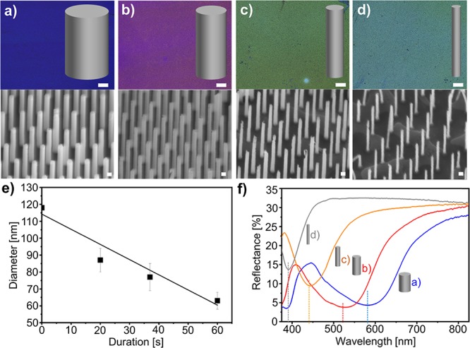
Control of SiNW diameter via KOH etching. (a–d) Top row: optical microscopy images of homogeneously etched silicon nanowire arrays using an aqueous 0.2 wt % KOH solution. Scale bars: 100 μm. Bottom row: secondary electron SEM images. Tilt angle: 30°. Scale bars: 100 nm. (a) Reference substrate after MACE, d = 118 nm. (b) SiNWs with d = 87 nm, after 20 s KOH etching. (c) SiNWs with d = 77 nm, after 40 s KOH etching. (d) SiNWs with d = 63 nm, after 60 s KOH etching. (e) Graph showing the wire diameter as a function of KOH etching duration. Pitch = 430 nm. KOH etching was performed immediately (i.e., within 30 s) after an HF pretreatment. (f) Reflectance spectra of the SiNW arrays shown in a–d. The characteristic minimum in reflection blue-shifts for smaller diameters. Photographs of the substrate and the area used for reflectance measurements can be found in Figure S2.