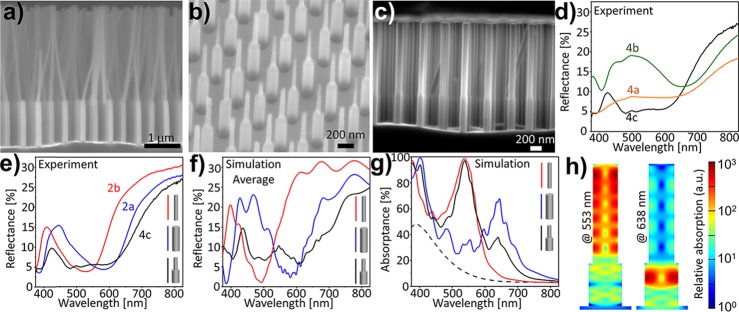
Figure 4.
Bisegmented nanowires via sequential MACE and KOH etching. (a–c) Secondary electron SEM images of different bisegmented VA-SiNW arrays. (a) Nanowires composed of a top segment with a high aspect ratio of 38 (dtop = 69 nm) and a bottom segment with a low aspect ratio of 9 (dbottom = 137 nm). The difference in aspect ratios leads to a selective bundling of the top part of the wires. (b) dtop = 60 nm and dbottom = 143 nm. (c) dexp,top = 98 nm and dexp,bottom = 133 nm. (d) Experimental reflectance spectra of the substrates shown in a–c. (e) Experimental reflectance spectra. Black curve: bisegmented VA-SiNWs shown in c. Red curve: single-diameter VA-SiNWs with dexp1 = 87 nm from Figure 2b. Blue curve: single-diameter VA-SiNW with dexp2 = 118 nm from Figure 2a. (f) Simulated reflectance spectra of arrays with similar dimensions as those used in e, same color code. The spectra were obtained by averaging the spectra over different diameters to take into account the wire size distribution (Table S5 for more details). (g) Simulated absorptance spectra of VA-SiNW arrays with different diameters but with the same volume, set by their length, to allow direct comparison of the simulated optical data, and highlighting the opportunity to control light absorption by engineering nanowires composed of segments with different dimensions. Black curve: dsim,top = 100 nm, dsim,bottom = 130 nm. Red curve: dsim1 = 100 nm. Blue curve, dsim2 = 130 nm. The corresponding simulated reflectance and transmittance spectra are shown in Figure S9. The dashed black line corresponds to flat silicon. (h) Two-dimensional maps of the simulated relative absorption within the bisegmented nanowires simulated in g at 553 and 638 nm.

