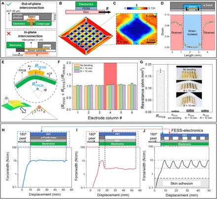
Fig. 2. FESS strain simulation and characterization of strain-isolated signal interconnection.

(A) Illustration of the FESS’ out-of-plane signal interconnection versus conventional in-plane signal interconnection. Conventional implementations are constrained to signal routing through highly strained regions, while the devised FESS allows for routing via near-zero strain regions. (B) COMSOL-simulated strain (ε) profile of a representative FESS in the presence of an externally applied shear force, illustrating near-zero strain at the bottom of the microchannel (i.e., substrate-biofluid interface). (C) Corresponding zoomed-in view of the strain profile for one “pixel.” (D) Strain distribution along the dashed line in (C). (E) Out-of-plane interconnection electrical characterization of FESS, performed under different localized bending angles (for an array of 6 × 6 Au electrodes). (F) Interconnection resistances of the bent FESS-FPCB (RFESS + RFPCB), for different localized bending angles (normalized with respect to RFPCB with no bending, RFPCB,0). Error bars indicate standard error of measurements across the six electrodes within each column. (G) Resistance measurements of the FESS electrodes under different bending angles (n = 36), in relation to the FPCB contact pad resistance (RFPCB,0). (H to J) 180° peeling tests characterizing the interconnection adhesion between the PCB and FESS with different backing structures: microfluidic base–ACF (H), microfluidic channel–ACF (I), and a representative microfluidic channel array–ACF (J). (Photo credit: Peterson Nguyen, University of California, Los Angeles.)
