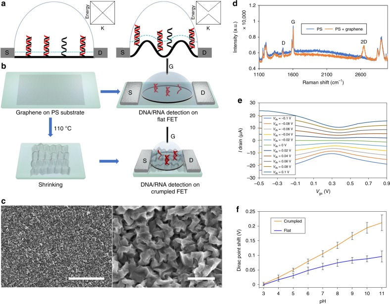
Fig. 1. Scheme and characterization of flat and crumpled graphene FET biosensor.
a Cross-sectional scheme of the flat (left) and crumpled (right) graphene FET DNA sensor. Probe (black) and target (red) DNA strands are immobilized on the surface of graphene. The blue dot lines represent Debye length in the ionic solution and the length is increased at the convex region of the crumpled graphene, thus more area DNA is inside the Debye length, which makes the crumpled graphene more electrically susceptible to the negative charge of DNA. The inset boxes represent qualitative energy diagram in K-space. Graphene does not have intrinsic bandgap. However, crumpled graphene may open bandgap, which is discussed in the later section and supplementary table 4. b fabrication of FETs and experimental process flow. Graphene on pre-strained PS substrate was annealed at 110 °C to shrink the substrate and crumple the graphene. Then source and drain electrodes were applied and solution-top gate was used. In case of flat graphene FET, the annealing process was omitted. c SEM images of crumpled graphene. The scale bar is 5 µm (left) and 500 nm (right). d Raman spectroscopy of crumpled graphene and PS substrate. e Charge transfer characteristics of the fabricated crumpled graphene FET. Vgs vs Ids (bottom) with the variation of Vds graphs showed shift in the Dirac point. f Dirac point shifts of the FET sensor plotted as a function of pH values. n = 5, mean ± std.

