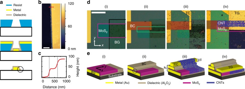
Fig. 1. Fabrication of Gaussian heterojunction transistors.
a Photolithography-based self-aligned fabrication, which is enabled by resist undercuts that are controlled by spin-coating speeds, exposure time, and development time. b Atomic force microscopy topography image of an electrode and dielectric extension (2 µm scale bar) corresponding to the dashed circle in a. c Height profile corresponding to the dashed red line in b, revealing a sub-exposure-wavelength extension of ~300 nm on monolayer MoS2. d Optical micrographs of the fabrication process (50 µm scale bar). e Three-dimensional rendering of the device structure throughout fabrication.

