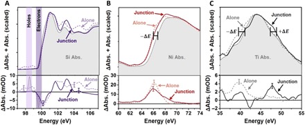
Fig. 2. Photoexcited changes in the Si, TiO2, and Ni separately and in a junction.

The differential absorption versus photon energy from Fig. 1C is plotted in the bottom row, while the top row shows the differential absorption scaled and added to the ground-state absorption. The solid lines represent the excited-state change for the elements in the junction for (A) Si 100 fs after photoexcitation, (B) Ni 100 fs after photoexcitation of the Si, and (C) TiO2 1 ps after the photoexcitation of Si. The same time differential absorption versus photon energy is shown for photoexcitation of each element alone as a dashed line. As discussed in the text, different excitation wavelengths and thicknesses were required to photoexcite the elements alone as compared to the junction. A representative error bar of the experimental few mOD noise is shown at key comparison energies.
