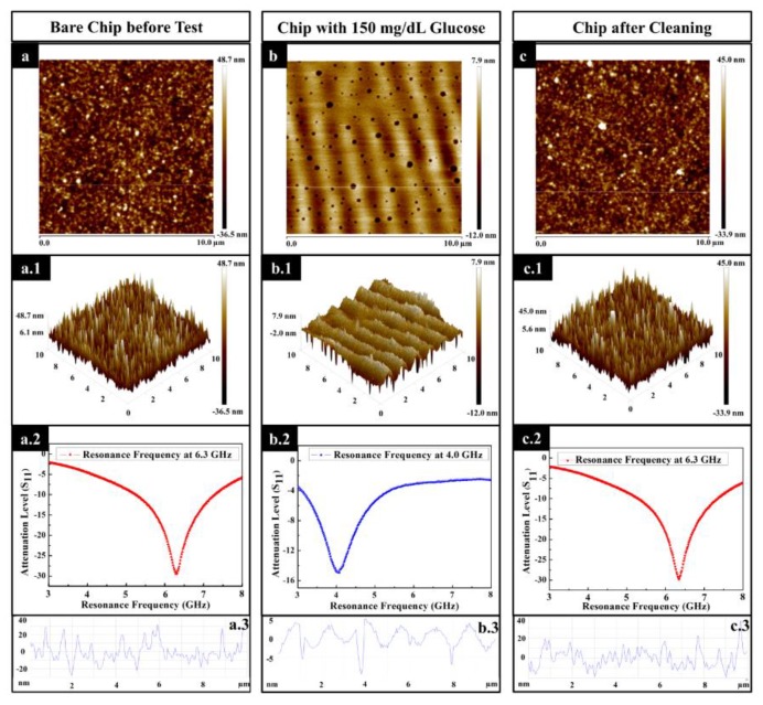
Figure 6.
The analysis for surface morphology of the sensing area. (a) The 2D view of bare biosensor, (a.1) the 3D view of bare biosensor, (a.2) the RF measurement of bare biosensor, and (a.3) the cross-sectional surface line profile of surface morphology for bare biosensor. Bare chip refers to the chip treated by a 3 min dry etching process. (b) The 2D view of biosensor with glucose concentration of 150 mg/dL, (b.1) the 3D view of biosensor with glucose concentration of 150 mg/dL, (b.2) the RF measurement of biosensor with glucose concentration of 150 mg/dL, and (b.3) the cross-sectional surface line profile of surface morphology for biosensor with glucose concentration of 150 mg/dL. (c) The 2D view of biosensor after cleaning, (c.1) the 3D view of biosensor after cleaning, (c.2) the RF measurement of biosensor after cleaning, and (c.3) the cross-sectional surface line profile of surface morphology for biosensor after cleaning.

