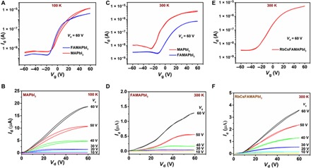
Fig. 1. Top-gate perovskite FETs fabricated by the antisolvent method—effect of channel length and cation composition.

(A) Transfer characteristics measured at 100 K on top-gate, bottom-contact perovskite FET fabricated from MAPbI3 (red) and FAMAPbI3 (blue) with L = 100 μm, W = 1 mm. (B) Output characteristics measured on the same MAPbI3 FET depicting a decrease in hysteresis compared to devices fabricated with L = 20 μm, W = 1 mm (figs. S1A and S2A). Transfer characteristics measured at 300 K on perovskite FET (L = 100 μm, W = 1 mm) fabricated from (C) MAPbI3 (red) and FAMAPbI3 (blue). (D) Corresponding output characteristics measured on FAMAPbI3 perovskite FETs with L = 100 μm, W = 1 mm. (E) Enhancement in the ON current in the transfer characteristics for FETs (L = 100 μm, W = 1 mm) fabricated with RbCsFAMAPbI3; the corresponding output characteristics (F) exhibit low hysteresis, but there is still some suppression of the current at small drain voltages, indicating sizable contact resistance.
