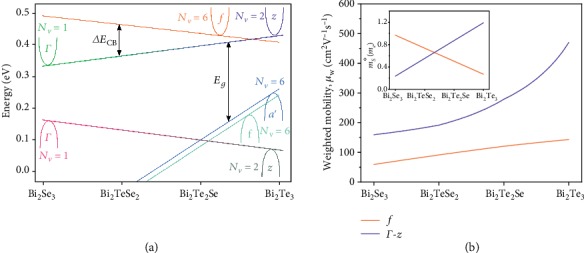
Figure 5.

(a) Four band edges are primarily responsible for the electronic transport in the n-type Bi2Te3−xSex alloy system. The peak in the conduction band Seebeck effective mass near Bi2Te2.7Se0.3 occurs due to the crossing of the sixfold f and twofold z valleys. The loss of weighted mobility with increasing selenium content is attributable to the reduction in effective valley degeneracy due to the f pocket rising far above the CBM and increasing in mass and the z pocket transitioning from Nv = 2 to 1 as the curvature inverts at Γ due to the reduction in SOI-induced anticrossing. The peak in band gap near Bi2Te2Se can be understood as a crossing between the a′ and Γ/z valence band edges. This schematic can be used to fit a two-band effective mass model with weighted mobility and effective mass parameters as shown in (b). These parameters generate the dashed lines fit to transport data in Figure 2.
