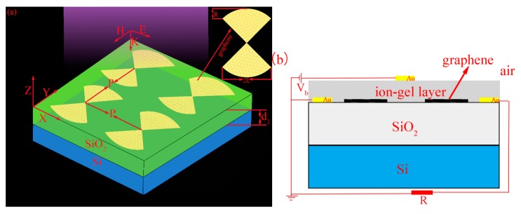
Figure 1.
(a) The schematic of “hourglass” graphene arrays structure with period (P), semimajor axis (L), semiminor axis (R). The two layers of substrate structure are Si and SiO2. The thickness of SiO2 is . (b) The side view of the structure which manipulates the chemical potential () of graphene by applying a voltage ().

