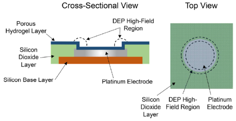
Figure 8.
Schematic of the microelectrode array chip showing the cross-sectional and top views of a single electrode. Over 1000 electrodes can be in a single device. The DEP high-field regions where particles are collected are shown within the dotted lines. The darker color of the silicon dioxide layer and electrode in the top view represents the overlying transparent porous hydrogel layer. DEP stands for dielectrophoretic. Reprinted with permission from Ref. 114. Copyright 2017, American Chemical Society.

