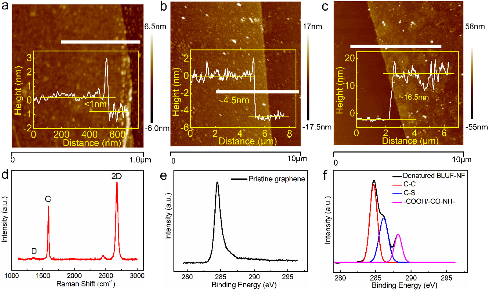
Figure 2.

The characterization results in the modification processes. (a) The AFM image of pristine graphene. Inset shows the thickness of pristine graphene is approximately 1 nm when measured along the horizontal white line in AFM image. (b) The AFM image of the thermal denatured BLUF-NF films on graphene surface. Inset shows the thickness of BLUF-NF layer is approximately 3.5 nm when measured along the horizontal white line in AFM image. (c) The AFM image of the the cross-linked BLUF-K5 films on graphene surface. Inset shows the thickness of BLUF-K5 layer is approximately 12 nm when measured along the horizontal white line in AFM image. (d) The Raman spectrum of pristine graphene. (e) The XPS C1s peak of pristine graphene. (f) The XPS C1s peak of the denatured BLUF-NF films on graphene surface.
