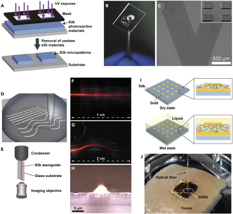
Figure 9.
Optical Elements of SF Materials
(A) Schematic of the fabrication of microstructures using silk protein lithography.
(B and C) An image and scanning electronic microscope (SEM) images of 10-μm squares patterned to form the “VCU logo"; scale bar: 500 μm. Reprinted with permission from Kurland et al., 2014. Copyright 2014, John Wiley & Sons, Inc.
(D–H) Schematic of (D) the direct-write assembly of silk waveguides and (E) the experimental setup. Optical images of (F) straight and (G) wavy silk waveguides guiding light from a He:Ne laser source. (H) Transverse image of the output face of a silk waveguide. Reprinted with permission from Parker et al., 2009. Copyright 2009, John Wiley & Sons, Inc. Scaling bars indicate 1 cm (in F), 2 cm (in G) and 5 μm (in H), respectively.
(I and J) (I) Schematic of the working principle of the silk plasmonic absorber sensor (SPAS) and an image of an SPAS on chicken breast tissue. Reprinted with permission from Lee et al., 2015. Copyright 2015, American Chemical Society.

