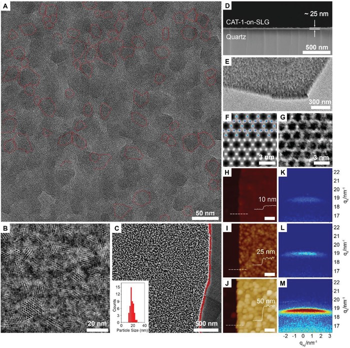
Figure 2.

Direct visualization of the vertically aligned and densely packed Ni‐CAT‐1 film on the graphene layer. A) High‐resolution TEM image reveals the majority of the Ni‐CAT‐1 crystals are collectively aligned with their c axis perpendicular to the graphene layer. The average crystal domain size of Ni‐CAT‐1 is 20 nm. B) Integrated differential phase contrast (iDPC) STEM image. C) SEM image of Ni‐CAT‐1‐on‐SLG. The silicon substrate, graphene, and the MOFs are clearly observed, with the edge of graphene layer marked in red. D) SEM image of Ni‐CAT‐1‐on‐SLG‐25 nm construct in cross‐section view. E) TEM image at rotated angle in relatively low magnification. F) Symmetry averaged STEM image obtained by using the fast Fourier transfer (FFT) data extracted from HAADF image. Inset is the structure model of Ni‐CAT‐1 which is in good agreement with the STEM image. G) Zoomed‐in iDPC STEM image of a single Ni‐CAT‐1 crystal domain. H–J) AFM images of Ni‐CAT‐1‐on‐SLG, which gives the thickness of the MOF layer. The domain size also increases as the thickness increase. Scale bar is 200 nm. K–M) GI‐SAXS data of the corresponding Ni‐CAT‐1‐on‐SLG constructs with zoomed‐in region of 004 reflections. The narrow spread width of 004 peaks reveals the epitaxial growth of Ni‐CAT‐1 on SLG.
