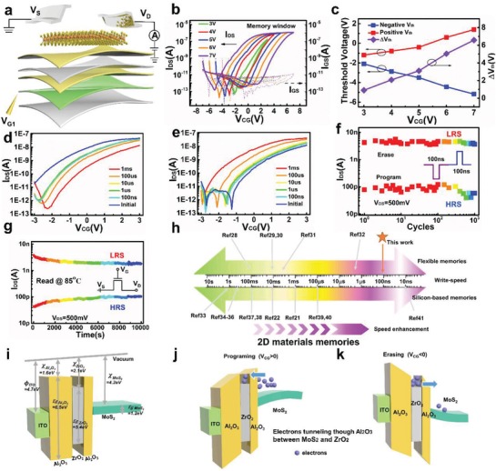
Figure 2.

Device characteristics and band diagram of the ultrafast flexible MoS2 memory. a) Schematic illustration of device structure for electrical measurement. b) Transfer characteristics of MoS2 memory under different V CG sweeping ranges (3, 4, 5, 6, and 7 V) and V DS = 500 mV. c) Memory window extracted from transfer curve with large hysteresis. d) Program and e) erase speed of device demonstrated using different pulse width of V CG (1 ms, 100 µs, 10 µs, 1 µs, 100 ns) after initialization (V CG = ±6 V, 1 ms). f) Endurance characteristics of the flexible MoS2 memory for 1000 cycles under programming (8.5 V, 100 ns) and erase (−7 V, 100 ns) operations at room temperature, where V DS = 500 mV. g) Retention behavior of device after programming and erasing with a 100 ns pulse, where V DS = 500 mV. h) Comparison of operation speed of 2D material memories with silicon and flexible substrates. i–k) Schematic band diagram of the MoS2 memory under i) flat band state, j) program operation (V CG > 0), and k) erase operation(V CG < 0). Φ, χ, and E g represent the work function, the electron affinity, and band gap, respectively.
