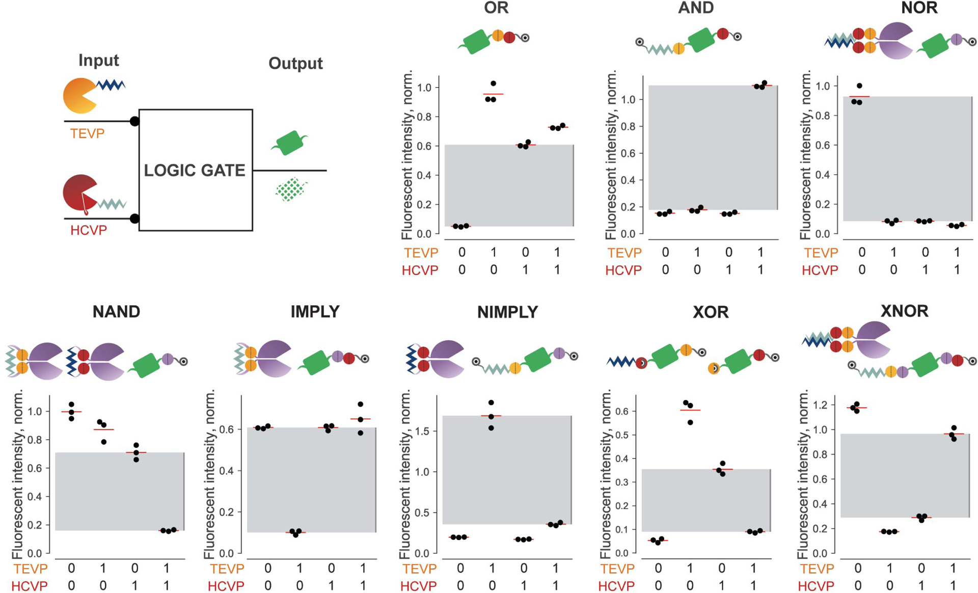
Fig. 2. CHOMP circuits implement binary logic gates.

For each indicated gate, TEVP and HCVP serve as binary inputs, which are either included or excluded in transfections. Citrine fluorescence serves as gate output. The design and performance of each nontrivial two-input logic gate is shown for triplicate experiments (black dots). Fluorescence intensity in each panel is normalized to the corresponding reporter stabilized with TMP (for gates containing only C-terminal degrons) or Shield-1 plus TMP (for gates containing degrons at both termini). Gray regions indicate the range from maximum “OFF” value to minimum “ON” value for that gate.
