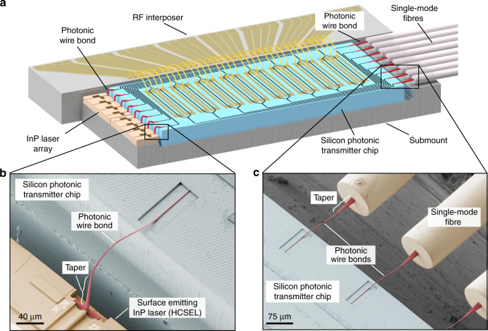
Fig. 1. Concept and implementation of hybrid multi-chip modules (MCMs) by 3D nano-printing of photonic wire bonds (PWBs).
a Illustration of an eight-channel transmitter, realized as a hybrid MCM comprising 3D-printed PWBs shown in red. PWBs allow efficiently connections between photonic integrated circuits (PICs) that are realized on different integration platforms, thereby combining the complementary strengths of the underlying material system. The illustrated transmitter combines efficient InP lasers with electro-optic modulators on a silicon photonic chip. The modulator array is electrically driven via an RF fan-in and connected to an array of single-mode fibres. b Interface between an InP laser chip and the silicon photonic transmitter chip. The light source is realized as a horizontal cavity surface emitting laser (HCSEL), consisting of a waveguide-based optical cavity in the substrate plane and an etched 45° mirror that redirects the light towards the substrate-normal direction17. c Fibre-to-chip interface. For efficient coupling to the large mode-field of the SMF, the PWBs are designed to have a larger cross section towards the fibre facet. The 3D freeform trajectory of the PWBs is adapted to the exact position of the corresponding interfaces and thereby replaces high-precision active alignment of the chips

