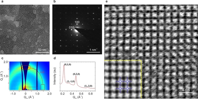
Figure 5.

a) TEM image showing the increased average domain size up to ≈150 nm. b) SAED pattern of a single‐crystalline domain along the [001] direction of PI‐2DP 1. c) GIWAXS image of PI‐2DP 1 on 300 nm SiO2/Si. d) In plane projection of GIWAXS data from (c). e) HRTEM image showing the square lattice with significantly reduced distortion (Inset: simulated HRTEM image with the atomic model overlaid, the porphyrin units appear bright, Figures S9 and S10).
