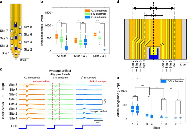
Fig. 4. Location dependence of residual artifact.
a Schematic illustration of the tip of shielded μLED optoelectrode. b The peak-to-peak magnitude of highpass filtered stimulation artifact recorded on shielded μLED optoelectrodes with different substrate doping densities. Data from channels corresponding to electrodes on the shank on which an LED was turned on are plotted. LED drive signal with resulting LED surface irradiance of 75 mW mm–2 was used. Boxes indicate interquartile ranges, white lines medians, whiskers non-outlier extreme values, and black x marks outliers. c Mean waveforms of stimulation artifact recorded on the shielded μLED optoelectrodes with different substrate doping densities, from channels that correspond to electrodes on different locations on the tips. Shaded regions show one standard deviation away from the mean. LED drive signal with resulting LED surface irradiance of 75 mW mm–2 was used. d Magnified view of the region inside the rectangle with the black dashed lines on part a. The distances between the center of the interconnects and the center of an LED are shown. e Peak-to-peak magnitudes of highpass filtered stimulation artifact recorded from different channels on shielded μLED optoelectrodes with heavily boron-doped silicon substrate (miniSTAR optoelectrodes). LED drive signal with resulting LED surface irradiance of 75 mW mm–2 was used. A detailed description of the samples, statistical tests used, and the results of statistical tests are provided in Supplementary Table 2.

