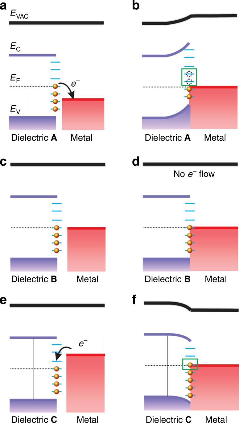
Fig. 5. Electronic quantum transition model of contact-electrification between a dielectric and metal.

a When a dielectric A is brought into contact with the metal as shown in the figures, some electrons on the surface states flow into metal to seek the lowest energy states. b The energy bands bend to align the Fermi levels. Most electrons at the surface energy states above the balanced Fermi level flow into metal and left an equal amount of holes at the surface (as shown in green box). Thus, the original neutrally charged dielectric A turns to have positive charges on the surfaces due to the electrons lose. c, d When a dielectric B is brought into contact with the metal, the Fermi levels are balanced, the surface energy states equal. There are no quantum transitions between the two materials. e When a dielectric C contacts the metal, electrons on the surface of the metal flow into the dielectric C to seek the lowest energy levels. f The energy bands shift to align the Fermi levels. Electrons flow from metal to dielectric C to fill the empty surface states due to the difference of energy levels (as shown in the green box). The original neutrally charged dielectric C turns to carry negative charges on the surfaces by obtaining electrons.
