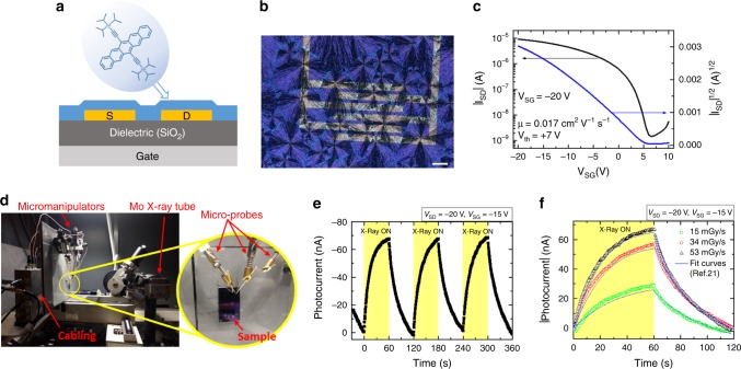
Fig. 1. BAMS deposited TIPS-pentacene OFETs as X-ray detectors.
a Schematic representation of the bottom-gate bottom-contact OFETs employed in this work, showing the cross section of the devices and the molecular structure of TIPS-pentacene. b Cross-polarized optical microscope image of a pure TIPS-pentacene thin film deposited by BAMS on a Si/SiO2 substrate with pre-patterned interdigitated electrodes. Scale bar is 100 µm. c Typical transfer characteristics in the saturation regime of a pure TIPS-pentacene OFET. d Photograph of the experimental setup for the samples irradiation with a Mo-target X-ray tube. e X-ray induced photocurrent response of a pure TIPS-pentacene BAMS-coated device upon three on/off switching cycles (yellow areas, time windows of 60 s) employing a dose rate of 53 mGy s−1, reaching a high sensitivity value of 3.8 · 102 µC Gy−1 cm−2. f Experimental and fitted curves of the response of the same device for three different dose rates of radiation yielding an amplification of the photocurrent of 2 · 106. The fit curves have been obtained by applying the analytical model described in ref. 21.

