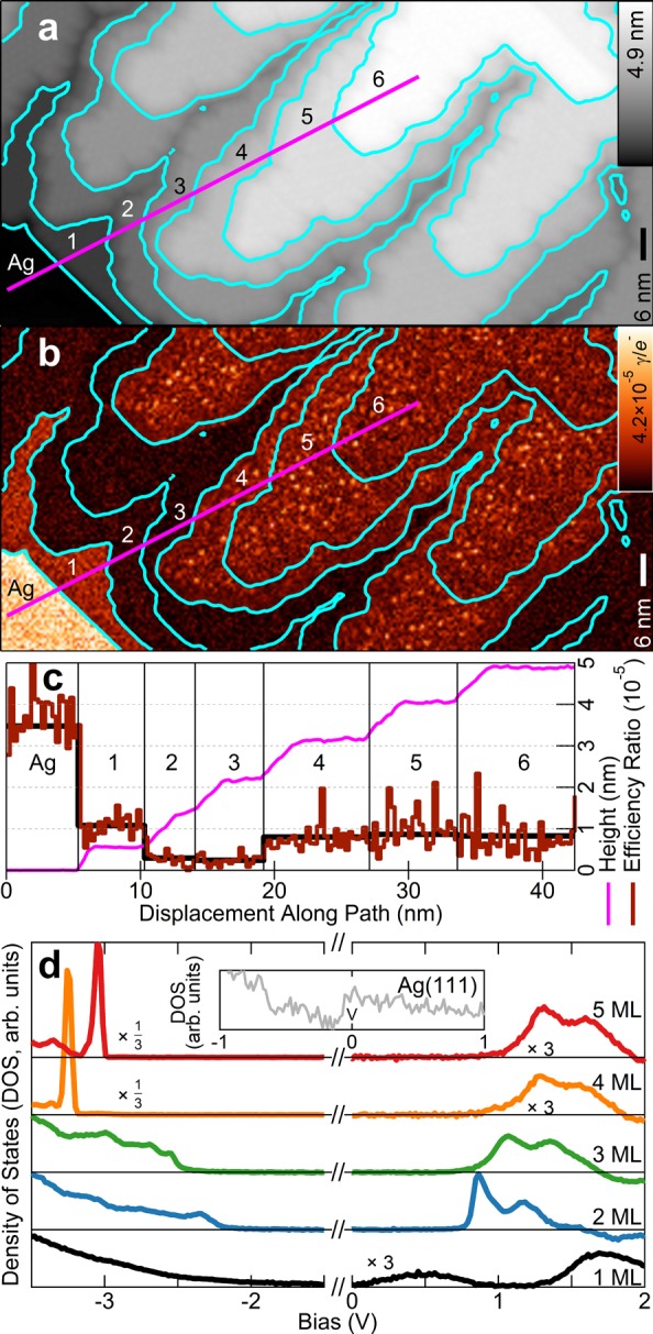
Figure 3.

STML surface characterization of C60-Ag(111). (a) Topography of a C60 film on Ag(111); U = −3.5 V, I = 20 pA constant current. (b) Light emission map, where γ/e– denoting photons per electron, is calculated as light intensity × elementary charge unit/current; same set point as (a). (c) Line profiles of topography and emission efficiency along the magenta lines marked in (a) and (b), respectively. The thick black line follows the average efficiency value of each terrace. (d) Differential conductance (dI/dV) spectra of the substrate (inset) and of 1–5 ML C60 atop this substrate, with spectra shifted vertically for clarity; set point U = −3.5 V, I = 100 pA.
