Figure 4.
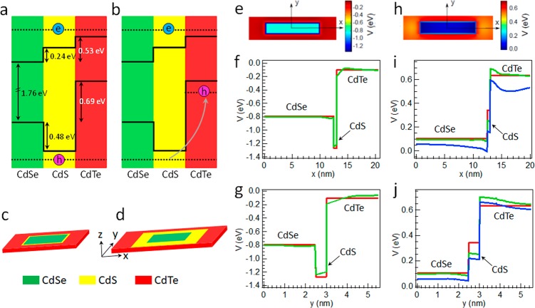
(a, b) Conduction and valence band alignment in the CBC heterostructure, considering unstrained band offsets. (a) A hot electron–hole pair is created. (b) The hole relaxes faster than the electron, conditioning the potential landscape that the hot electron sees at the moment of relaxation. (c, d) Schematic of the CBC NPLs under study, resembling Batch3 with a narrow CdS barrier (c) and Batch4 with a wider barrier (d). (e–g) Potential landscape seen by a photoexcited valence band hole for a narrow-barrier sample, with a 2D in-plane cross section (e) and 1D profiles along x- (f) and y- semi-axes (g), as depicted in (e). In the 1D plots, red and green lines show the potential excluding and including the influence of strain. The origin of energies is taken at the top of the CdTe band. (h–j) Same as (e–g) but for conduction band electrons. Blue lines in (i) and (j) panels show the potential including the Coulomb attraction exerted by the hole ground state localized in the CdTe crown. The origin of energies is taken at the bottom of the CdSe band.

