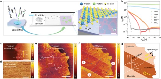
Figure 1.

Synthesis of semiconducting V‐doped monolayer WSe2 and ferromagnetic characteristics. a) Schematic of synthesis of V‐doped WSe2 by mixing liquid W with V precursors. The inset shows optical image of CVD‐grown V‐doped WSe2 monolayer. Scale bar, 50 µm. b) Source‐drain current (biased at 1 V) with the gate bias for V‐doped WSe2 field‐effect transistors with various V‐doping concentrations. c) Topography and d) MFM phase images of pristine WSe2 at RT. Scale bar, 10 µm. e) Topography and f) MFM phase images of 0.1% V‐doped WSe2 at RT. Scale bar, 10 µm. g) The schematic typical features observed in MFM phase images.
