
Figure 2.
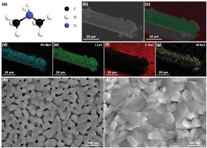
Characterization of the Syn‐PbI2 Powder and the Corresponding Syn‐CsPbI3 film. a) Molecular structures of DMA+; b) SEM image; c) EDS mapping of N, Pb, and I; d–g) EDS mapping of d) Pb element, e) I element, f) C element, and g) N element distribution; and SEM image of h) unannealed and i) annealed syn‐CsPbI3 film.