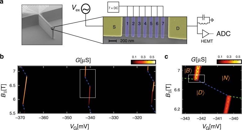
Fig. 2. Experimental setup and transport signature.
a Scanning electron microscope image of the device: At the edge of an etched cantilever, a nanotube is positioned on two contacts (S,D) and suspended over a piano of seven gates. The conductance through the device is measured with an AC excitation on S (Vex at ~1.5 MHz) and a cryogenic LC tank circuit connected to the drain (D) followed by a cold HEMT amplifier. b Measured conductance, G, as a function of gate voltage common to all seven gates, VG, and B||, exhibiting a zig-zag of bright and dark charging lines (the latter marked by dashed blue). c Zoom-in on one triple point, with the schematic lines separating the , and states are marked as in Fig. 1c.

