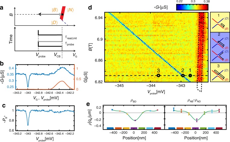
Fig. 4. Time domain measurements of the qubit transition.
a Measurement sequence, plotted in gate voltage–B|| plane (top) and in gate-voltage time diagram (bottom). The state is initialized on the ↔ Coulomb blockade (CB) line (red, star marks initialization point). Voltage on the center three gates is rapidly ramped to a value Vprobe, dwelling a time τprobe, and then ramped back to the original point on the CB line, dwelling a time τread,init. The sequence is repeated periodically. b Conductance averaged over the above sequence, , measured as a function of Vprobe (blue) and the quasi-DC conductance, G(red), measured at the same point in VG. c Bright state return probability, as a function of Vprobe, determined from and G in panel b (see text). d Similar measurement of but now as a function of Vprobe and B||. A red peak is visible at the location of the Coulomb blockade peak and a much narrower blue dip appears along a line that corresponds to the ↔ crossing. Both a fast traverse to a point before this line (marked 1) or after this line (marked 3) do not alter the state of the system from its initialized state, however, a fast traverse to a point on the line (marked 2) results in occupation of the state with a significant probability. The corresponding traverses in energy are shown in the side panels. e Left: The change in spatial charge distribution at the ↔ transition, ρBD(x), imaged using gate resolved capacitance shift imaging of this line (as outlined in Fig. 3a). Right: The difference between the the spatial charge distributions measured at the ↔ and ↔ transitions, ρNB(x) − ρND(x), taken from Fig. 3c and d, strongly resembling the directly imaged ρBD(x) in the left panel, further confirming that the narrow line corresponds to the ↔ transition.

