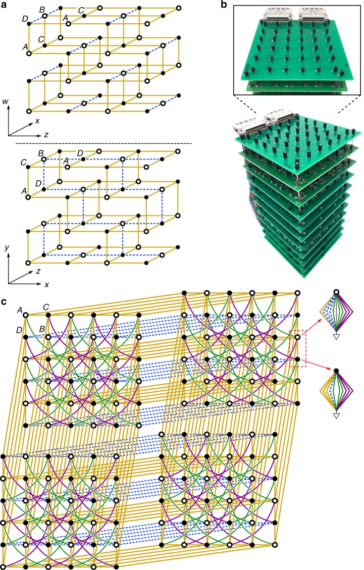
Fig. 1. Model of the 4D Quantum Hall lattice and its circuit implementation.
a Schematic of the 4D tight-binding model. Each unit cell consists of four sites labelled A–D. Hollow and filled circles respectively denote positive (m) and negative (−m) on-site masses, while yellow solid lines and blue dashes respectively denote positive (J) and negative (−J) hoppings. b Photographs of the circuit. c Schematic of the circuit; positive (negative) masses are realised by capacitors (inductors) connecting the sites to ground, and hoppings are realised using capacitors or inductors connecting different sites. The components shown here are C0 = 1 nF (yellow lines), L0 = 2 mH (blue dashes), (purple curves), (green curves), and Cm = 2mC0 (grey dashes). Each site is grounded by a set of additional circuit components (see Supplementary Note 2); for clarity, only the grounding components for two sites (in the dashed red box) are depicted.

