Figure 2.
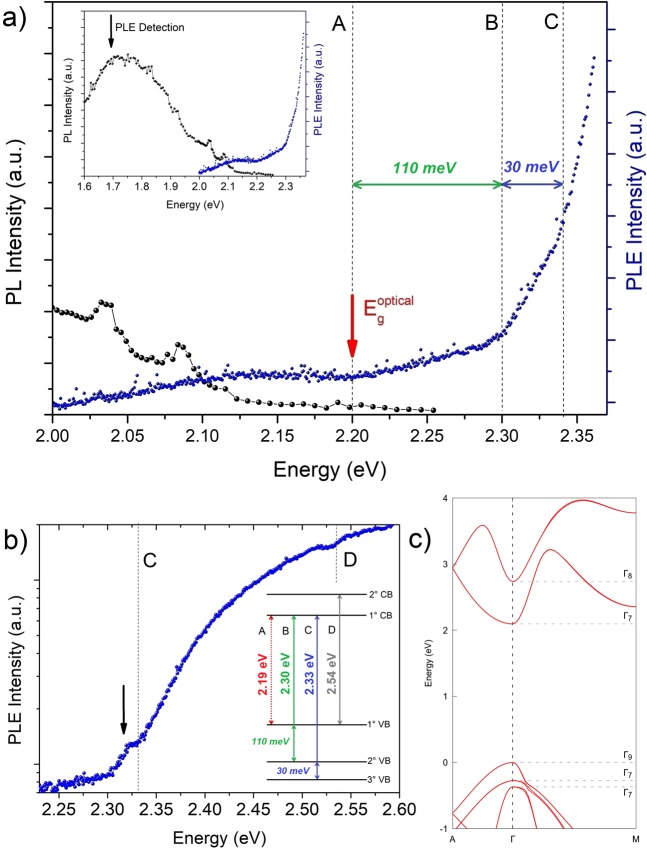
(a) PL and PLE spectra of the GaP structures performed at 10 K; dashed lines indicate the absorptions edges labeled A, B and C. Inset: the same PL and PLE spectra showed in (a) with broad range. The black vertical arrow indicates the detection position at 1.68 eV, used in PLE measurements. PLE was acquired using the maximum of the Xe lamp single monochromator aperture slit (2 mm) and a long integration time, in order to increase the signal/noise ratio of the ground absorption edges. (b) PLE performed with Xe lamp single monochromator aperture slit of 0.75 mm; additional absorption edge was observed at high energy and labeled D. The black arrow indicates the excitonic peak observed for transition C. Inset: schematic representation of the first absorption edges observed in PLE measurements. Dashed (solid) lines indicate the weak (strong) absorption edges with monotonic (parabolic) increase with energy. (c) Electronic band structure of the WZ GaP calculated by DFT method using HSE06 functional, implemented in the Vienna ab initio simulation package (VASP)15,16, version 5.4.4.

