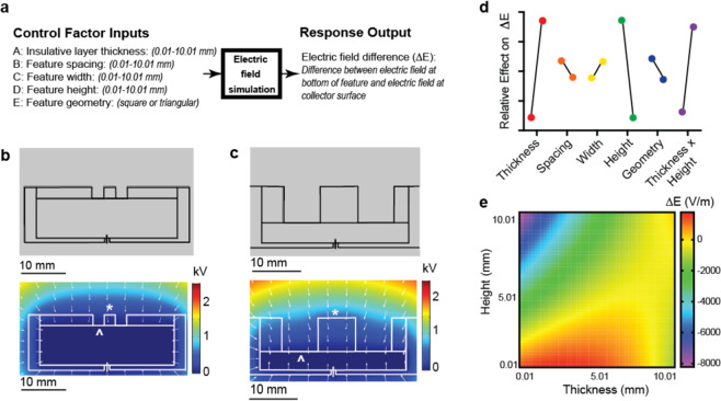
Figure 2.
Finite element method simulations following statistically designed experiments for collector geometry designs. (a) P-diagram of the design of experiments, including the five different control factor inputs and the primary response output. Factors were varied from 2.51 mm to 7.51 mm in the initial full factorial design, then were varied from 0.01 mm to 10.01 mm for the central composite design. Representative images from two distinct simulations for square feature geometry with (b) 2.51 mm width, height, spacing, and thickness, and (c) 7.51 mm width, height, spacing, and thickness. These images show the starting geometry, the calculated electric potential (color gradient, scale in kV), and electric field (arrow vectors). Annotations indicate the location of the collector surface (*) and bottom of the pattern (^) used to calculate the ΔE response output. (d) Means plot showing the relative effect of each factor at each level. The largest effect was observed for the insulative layer thickness, feature height, and the interaction of these two factors. (e) The heat map of ΔE from the quadratic model indicates that ΔE is maximized by limiting feature height to 5 mm and increasing the insulative layer thickness proportionally with increasing feature height.

