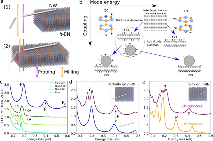
Figure 1.
(a) Samples consisting of silver nanowires deposited on h-BN were investigated with two different configurations: (1) nanowires partially supported by h-BN with one of their ends in vacuum; and (2) nanowires fully supported on h-BN. High-current (∼10 μA at 200 keV, orange) and low-current (∼10 pA at 60 keV, purple) electron beams were used for milling and probing, respectively. (b) Sketches of the different phonons, plasmons, and hybrid excitations discussed in the text. (c) Spectra of a 3.3 μm long metallic nanowire in vacuum (blue) and h-BN (green). The in-vacuum nanowire exhibits equally spaced surface plasmon modes labeled P. h-BN spectra are shown for the electron beam placed outside the material (aloof configuration), as well as thin and thick h-BN, where the FKS and FKA modes are observed. (d) Spectrum of a metallic nanowire in sample configuration (1) measured on the tip in vacuum (upper curve). The dipolar mode at ∼200 meV is split into two peaks compared with the nanowire in vacuum (lower curve). (e) Spectra for a metallic nanowire in configuration (2) under off- (orange) and on-resonance (purple) conditions.

