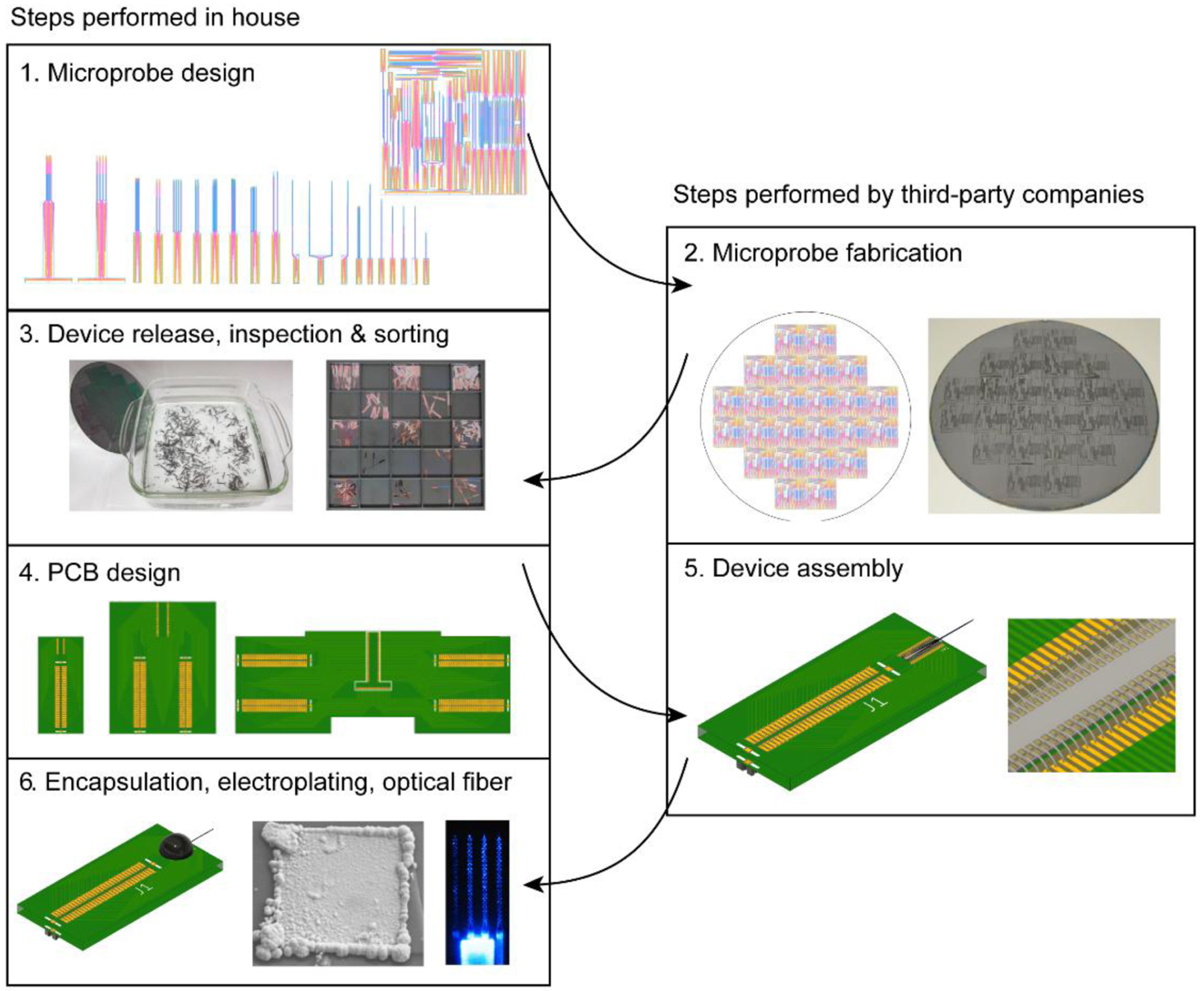
Figure 1. Overview of the main steps involved in silicon microprobe development.

The numbered steps on the left side are performed in house or by the end user, while the steps on the right side are performed by third-party companies. Step 1 shows CAD drawings of the individual probes and reticle. Step 2 shows the reticle copied multiple times across a wafer, and a photograph of a processed wafer. Step 3 shows hot water release of the probes from the carrier wafer, and sorting the devices by design into trays for storage. Step 4 shows the three standard PCB designs. Step 5 shows a probe assembled onto a PCB with wire bonding. Step 6 shows an assembled probe with epoxy encapsulation, a gold-plated electrode, and an opto-microprobe.
