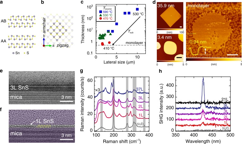
Fig. 1. Characterization of few-to-monolayer SnS.
a Cross-sectional crystal structures of SnS along the armchair direction with different stacking sequences: non-centrosymmetric AA and centrosymmetric AB staking. b Top view of crystal structure of monolayer SnS, whose twofold axis is along the armchair direction. Highlighted area shows thermodynamically stable facets. c The minimum thickness versus lateral size of PVD grown SnS with changing Tsource and Tsub. d AFM topographic images of SnS crystals with different thicknesses from bulk to monolayer. The scale bars represent 1 µm. e Cross-sectional bright-field STEM image of trilayer SnS. f Cross-sectional TEM image of monolayer SnS along the armchair direction. As guide to the eye, all of the region except the SnS crystal is shaded, and the atomic model is overlaid on the TEM image. g Thickness dependence of Raman spectrum for SnS at 3 K. The peaks in the hatch come from the mica substrate. h SHG spectra for SnS with different thicknesses from bulk to monolayer at RT.

