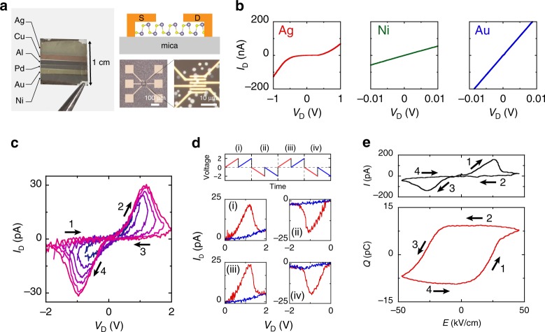
Fig. 4. Ferroelectric switching behaviors of few-layer SnS.
a Left: Photograph of mica substrate after the deposition of various metals with different work functions. Right: Cross-sectional schematic and optical images of two-terminal SnS devices. Typical channel length lch and width wch were lch = 0.4–0.8 µm and wch = 3–5 µm, respectively. b ID–VD curves for bulk SnS with different metal contacts: Ag, Ni, and Au. c RT ID–VD for Ag/9L-SnS device with different VD sweep ranges. VD was swept from minus to plus to minus (e.g., −1 → +1 → −1 V). d Double-wave measurement from 0 to 2 and 0 to −2 V. Top: applied voltage along time. The voltage was applied two times at the positive and negative bias repeatedly. Bottom: ID–VD curves for different sweeps (i)–(iv). The red and blue lines represent the first and second sweep, respectively. e Ferroelectric resistive switching for Ag/SnS: current and charge versus nominal electric field measured by ferroelectric measurement system at 1 Hz and RT.

