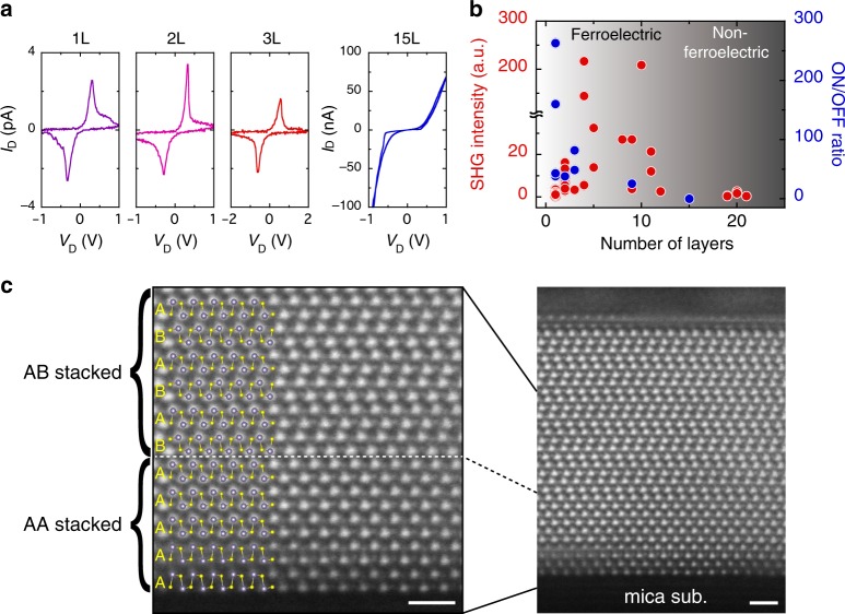
Fig. 5. Transition of stacking sequence from AA to AB staking.
a Ferroelectric resistive switching for SnS with different thicknesses: monolayer, bilayer, trilayer, and 15 L. b Thickness dependences of the SHG intensity and ON/OFF ratio for different thicknesses. The ON/OFF ratio was determined at the coercive electric field of ID–VD for Ag/SnS device. Each data points of SHG and ON/OFF ratio represent an individual SnS crystal. c Cross-sectional HAADF-STEM image of 16 L SnS along the armchair direction. The scale bars represent 1 nm.

