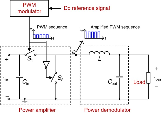
Fig. 2. Structure of a buck/boost converter.

S1 and S2 are two identical metal-oxide-semiconductor field-effect transistors (MOSFETs) as ideal switches, Cin denotes the input capacitor and Cout denote the output capacitor. L denotes the inductor. vin and vout are input and output voltages, respectively. The buck/boost converter can be divided into five components, as labelled in red: a dc reference signal, a PWM modulator, a power amplifier, a power demodulator, and a load. The power amplifier includes an input dc source and two switches operating in a complementary mode. The power demodulator includes an LC LPF. The waveform at point ‘e’ is the amplified PWM sequence.
