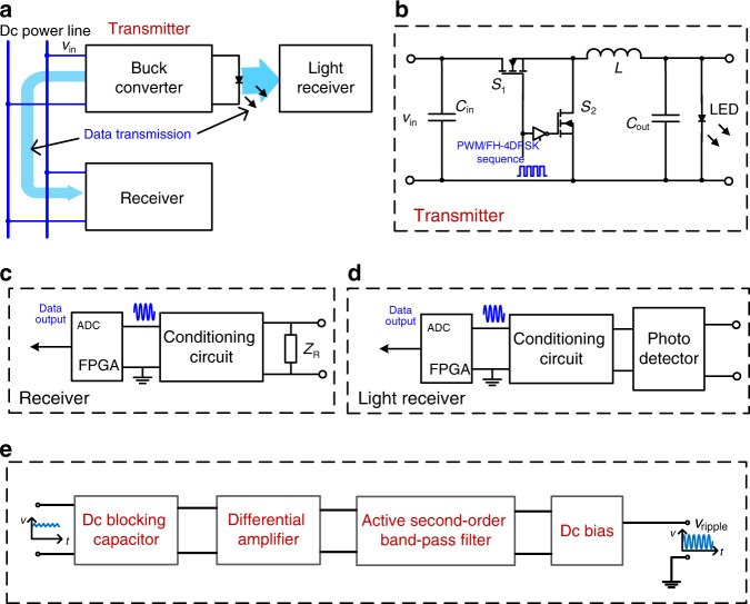
Fig. 9. Structure of the prototype LED lighting system.
In this experiment, PWM/FH-4DPSK modulation are employed. a The general structure of the experimental prototype, which includes a buck/boost converter as a data transmitter, a receiver sharing a common power line with the buck/boost converter and a light receiver. vin denotes the input voltage of the buck converter. Data are transmitted from the buck/boost converter to the receiver via the dc power line and to the light receiver via the visible LED light. b Detailed buck/boost converter circuit, in which vin denotes input voltage, Cin and Cout denote input and output capacitors respectively, and L denotes the inductor. The PWM/FH-4DPSK modulated signal is employed as the gate signal for MOSFET S1, and its complementary signal is the gate signal for MOSFET S2. c The structure of the receiver. It consists of an impedance ZR, a signal conditioning circuit and an FPGA with ADC to output digital data. d The structure of the light receiver, which consists of a photodetector, a signal conditioning circuit and an FPGA. e The signal conditioning circuit used in both the receiver and the light receiver. This circuit is composed of a dc blocking capacitor, a differential amplifier, an active second-order band-pass filter and a dc voltage bias circuit. The input signal is conditioned, and at the output port, the fundamental component of the switching ripple with a proper dc bias is obtained, denoted by vripple.

