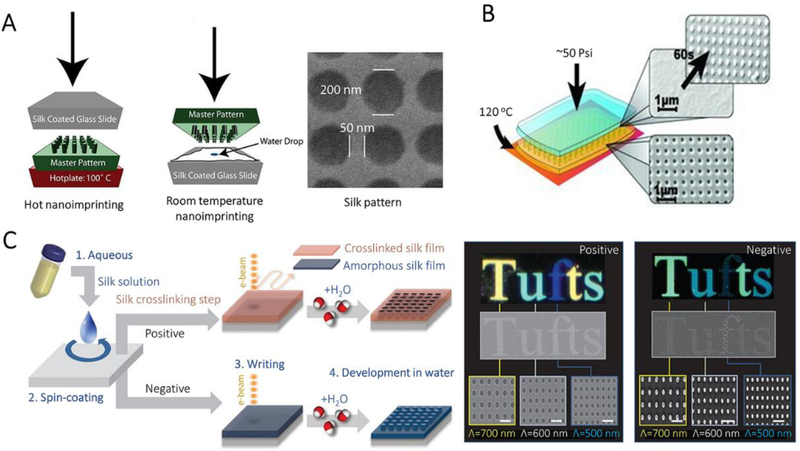
Figure 7.
Nanoimpriting and electron-beam patterning for the manufacture of SF nanostructures. A, Schematics of two nanoimprinting processes: hot embossing and room-temperature embossing. AFM and SEM images of period patterns in SF film. Reproduced with permission.[50] Copyright 2010, Wiley-VCH. B, Schematics of the protein-protein imprinting process and the corresponding SEM images showing the patterns of crystallized SF master (yellow) and imprinted amorphous SF (blue). Reproduced with permission.[51] Copyright 2013, Wiley-VCH. C, Schematic of all-water-based electron-beam patterning on a SF film. Dark-field and electron microscopy images of SF nanostructures generated on the positive and negative resist. Scale bars, 1 μm. Reproduced with permission.[52] Copyright 2014, Springer-Nature.

