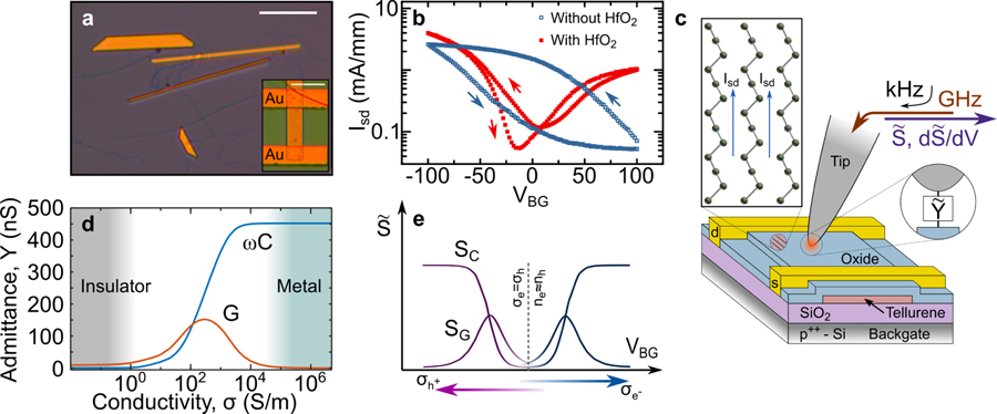
Figure 1:
(a) Optical micrograph of solution-grown tellurene crystals showing characteristic trapezoidal shape as well as string-like Te filaments formed during process (scale bar: 20 µm). Inset: Optical micrograph of a tellurene device (scale bar: 8 µm). (b) Transport characteristics of a tellurene FET before and after deposition of a 10 nm conformal HfO2 overcoat. (c) Schematic of the experimental setup illustrating the transport along the direction of the atomic Te chains. (d) Finite element modeling of the complex-valued tip-sample admittance at 17.3 GHz as a function of tellurene conductivity. (e) Illustration of the expected measured microwave signal as a function of VBG for an ambipolar FET showing clear regimes of contrast corresponding to hole- and electron-conductivity.

