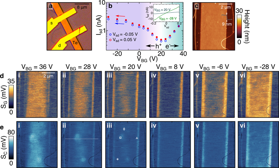
Figure 2:
(a) Optical micrograph of an Al2O3-encapsulated tellurene device with source and drain electrodes as indicated. (b) Transport characteristics of the device, with the global device carrier equivalence point at VBG = 20 V and electron and hole transport regimes as indicated. Inset: The IV characteristics of the device at VBG as indicated with near-ohmic behavior, though some nonlinearity and increased noise are seen at positive Vsd. (c) Contact mode AFM topography of the device active area (source and drain electrodes are just out of view at image top and bottom). (d) and (e) show SMM images acquired at sequentially decreasing values of VBG as indicated, with the conductance SG and capacitive SC channels, respectively.

